|
|
EIDORS: Electrical Impedance Tomography and Diffuse Optical Tomography Reconstruction Software |
|
EIDORS
(mirror) Main Documentation Tutorials − Image Reconst − Data Structures − Applications − FEM Modelling − GREIT − Old tutorials − Workshop Download Contrib Data GREIT Browse Docs Browse SVN News Mailing list (archive) FAQ Developer
Hosted by |
Viewing surface and depth voltagesCreate a simple 3D model (electrodes at 170° and 190°% Create fwd model el_pos = [190,0.5;170,0.5]; fmdl= ng_mk_cyl_models(1,el_pos,[0.05,0,0.05]); % Solve fwd model fmdl.stimulation(1).stim_pattern = [1;-1]; fmdl.stimulation(1).meas_pattern = [1,-1]; % dummy img = mk_image(fmdl,1); img.fwd_solve.get_all_meas = 1; vh=fwd_solve(img); clf;show_fem(fmdl); print_convert view_3D_surf01a.png '-density 75' 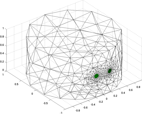
Figure: Cylinder with electrodes at 170° and 190° Show voltage on surface
imgv = rmfield(img,'elem_data');
imgv.node_data = vh.volt(:,1);

colours = calc_colours(imgv,[]);
patch('Faces',fmdl.boundary,'Vertices',fmdl.nodes, 'facecolor','interp', ...
      'facevertexcdata',colours,'CDataMapping','direct');

print_convert view_3D_surf02a.jpg '-density 75'
view(0,0)
print_convert view_3D_surf02b.jpg '-density 75'
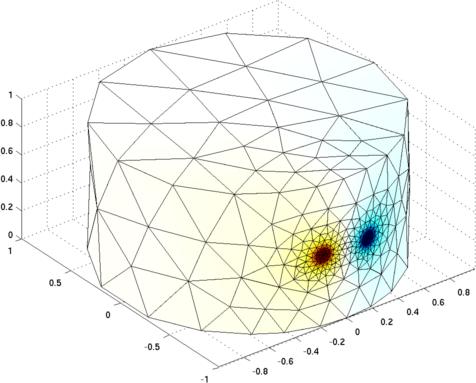 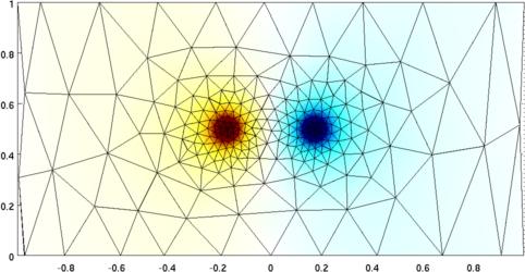
Figure: Two views of surface voltage on cylinder Show vertical slices (internal)% Four cut planes cut_planes = -[0.6;0.7;0.8;0.9]; imgv.calc_colours.backgnd = 0.9*[1,1,1]; show_slices(imgv,cut_planes*[inf,1,inf]); print_convert view_3D_surf03a.png '-density 150' 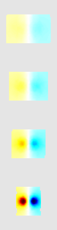
Figure: Vertical slices of internal voltage at 0.6, 0.7, 0.8, 0.9 Adding contrasts to adjust surface voltages
% Create fwd model
el_pos = [190,0.5;170,0.5];
extra = {'cube',['solid cube = orthobrick(-0.2 ,-0.97,0.6;0.2,0,0.7) or ' ...
                              'orthobrick( 0.15,-0.97,0.4;0.2,0,0.7) ;']};
fmdl= ng_mk_cyl_models([1,1,.05],el_pos,[0.05,0,0.05],extra);

% Solve fwd model
fmdl.stimulation(1).stim_pattern = [1;-1];
fmdl.stimulation(1).meas_pattern = [1,-1]; % dummy
img = mk_image(fmdl,1);
img.elem_data(fmdl.mat_idx{2}) = 10000;
img.fwd_solve.get_all_meas = 1;
vh=fwd_solve(img);

clf;show_fem(img);
print_convert view_3D_surf04a.jpg '-density 75'
view(0,0);
print_convert view_3D_surf04b.jpg '-density 75'
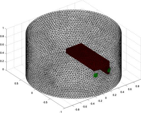 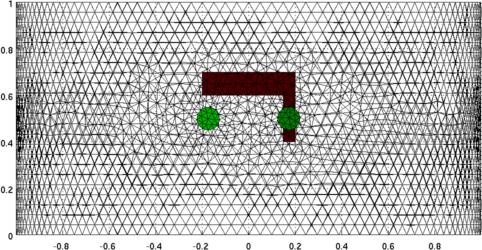
Figure: Cylinder model with contrasting region (higher mesh density to see details)
imgv = rmfield(img,'elem_data');
imgv.node_data = vh.volt(:,1);

imgv.calc_colours.clim = 0.3; % Colour limits
colours = calc_colours(imgv,[]);
show_fem(fmdl);
patch('Faces',fmdl.boundary,'Vertices',fmdl.nodes, 'facecolor','interp', ...
      'facevertexcdata',colours,'CDataMapping','direct');

view(0,0)
print_convert view_3D_surf05b.jpg
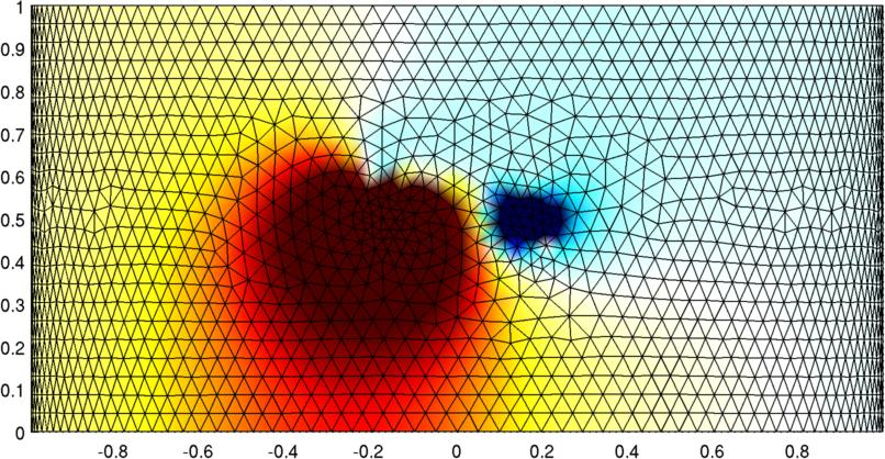
Figure: Two views of surface voltage on cylinder |
Last Modified: $Date: 2017-02-28 13:12:08 -0500 (Tue, 28 Feb 2017) $ by $Author: aadler $